Advancing Metal Additive Manufacturing Technology
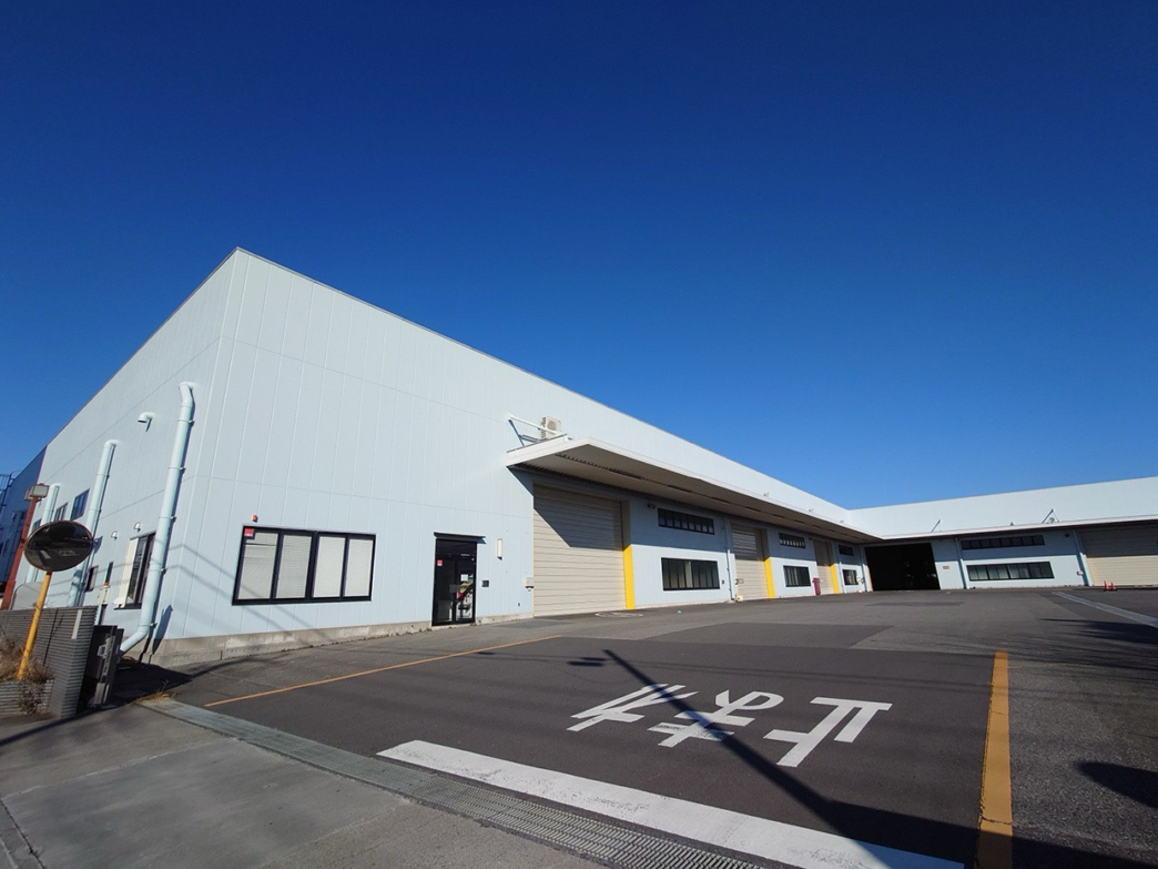
February 4, 2025 – Tokyo, Japan – Nikon Corporation (Nikon) has announced the launch of the Nikon AM Technology Center Japan in Gyoda, Saitama Prefecture. The facility will officially open on February 28, 2025, marking a significant step in Nikon’s Advanced Manufacturing initiative. The center is designed to accelerate the adoption of metal additive manufacturing (AM), offering cutting-edge solutions for industrial applications.
This expansion follows the July 2024 launch of the Nikon AM Technology Center in Long Beach, California, USA. The Gyoda facility will serve as a hub for AM research, development, and services in Japan and across Asia, reinforcing Nikon’s commitment to innovative digital manufacturing solutions.
Nikon AM Technology Center Japan: Key Features
The Nikon AM Technology Center Japan is equipped with state-of-the-art metal AM systems, including:
• NXG XII 600 Laser Powder Bed Fusion (L-PBF) system – The first of its kind in Japan, featuring 12 lasers and a large build platform capable of printing parts up to 1.5 meters.
• Lasermeister LM300A – A high-precision Directed Energy Deposition (DED) system, ideal for repair and sustainment applications.
• XT H320 X-ray CT Inspection System – Ensuring high-precision quality control for AM components.
• DfAM (Design for Additive Manufacturing) services – Providing customized design, prototyping, and metal mold optimization.
This facility will play a crucial role in the defense, aerospace, and industrial sectors, supporting Japanese and Asian manufacturers in adopting advanced AM solutions.
Expanding Nikon’s Advanced Manufacturing Vision
Nikon’s Vision 2030 strategy aims to establish the company as a global leader in technology solutions, where humans and machines collaborate seamlessly. With Digital Manufacturing as a key pillar of growth, the Nikon AM Technology Center Japan strengthens Nikon’s position in next-generation manufacturing.
Why This Matters:
• Accelerates AM adoption for defense, space, and aviation industries.
• Enables high-precision industrial manufacturing with state-of-the-art AM systems.
• Provides local AM solutions for Japanese and Asian businesses, reducing reliance on overseas production.
Nikon AM Technology Center Japan: Facility Overview
• Location: 1-7-1 Fujimi-cho, Gyoda City, Saitama Prefecture, Japan
• Opening Date: February 28, 2025
• Total Area: 922m²
• Key Equipment:
• NXG XII 600 (L-PBF system)
• Lasermeister LM300A (DED system)
• XT H320 X-ray CT system
• Main Services:
• Metal AM research & development
• Prototyping and production support
• Design for Additive Manufacturing (DfAM) services
Revolutionizing Metal Additive Manufacturing in Japan
The Nikon AM Technology Center Japan will drive innovation in metal 3D printing, enabling businesses to reduce production costs, enhance efficiency, and optimize designs. As Nikon continues to expand its Advanced Manufacturing portfolio, this facility will be instrumental in advancing high-precision, scalable AM solutions.
Stay updated with Nikon’s latest developments in metal additive manufacturing as they continue shaping the future of digital production technologies.
Source: https://www.nikon.com/company/news/2025/0204_01.html
